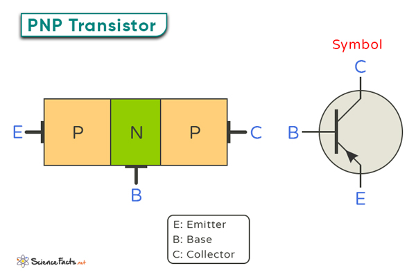
Symbol A PNP transistor is commonly represented in circuit diagrams using specific graphical symbols to denote its components and functionality. The emitter, represented by an outward arrow, indicates conventional current flow from the transistor. The base, situated centrally, controls the flow of current between the emitter and collector. It is denoted by a thin line intersecting the emitter arrow. The collector, opposite to the emitter, serves as the exit point for the current, symbolized by a bar perpendicular to the emitter arrow.
How Does a PNP Transistor Work
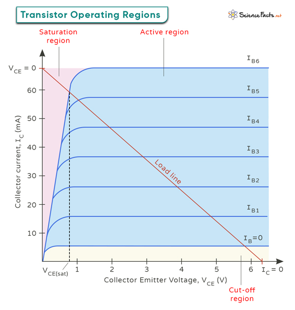
Operating Regions
Applications
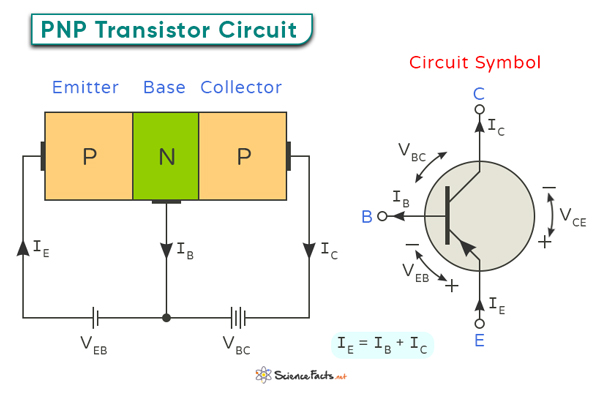
The forward bias at the emitter-base junction narrows the depletion region, allowing many holes to move from the emitter to the base. Conversely, the reverse bias at the collector-base junction widens its depletion region.
Current Flow
The movement of holes is responsible for the current flow in the PNP transistor. They enter the base from the emitter, where some recombine with electrons, necessitating the flow of base current (IB) to replace them. Since the base is thin and lightly doped, most holes pass through and reach the collector, creating the emitter current (IE). The remaining holes that do not recombine in the base continue to the collector, forming the collector current (IC). The relationship between IE, IB, and IC is as follows: IE = IB + IC
1. Cut-off Region
The cut-off region is when both the base-emitter and base-collector junctions are reverse-biased. In this state, the transistor is “off”, and no current flows between the emitter and collector, except for small reverse saturation currents. The cut-off mode is commonly used to ensure that a transistor remains inactive when not required to amplify or switch signals, thereby minimizing power consumption and preventing unwanted circuit behavior.
2. Active Region
The active region is where both the base-emitter and base-collector junctions are forward-biased. The voltage applied to the base terminal is sufficient to allow a moderate current to flow from the emitter to the collector. The transistor’s amplification capabilities come into play here, as small variations in the base current result in proportional changes in the collector current.
3. Saturation Region
Similar to the active region, both the base-emitter and base-collector junctions are forward-biased. In this region, the transistor conducts maximum current between the emitter and collector terminals, behaving essentially as a closed switch.